
Thin films for efficient light emission
Light emitting diodes (LEDs) are of great importance in modern technology. However, in the current market there are gaps in available wavelengths, particularly in the amber. Important research is being done toward creation of efficient emitters from AlInP alloys. In view of the desired application for light emission, a required property is to have the emission intensity as great as possible. Using other techniques, it had previously been observed that the PL intensity of AlInP films on AlGaInAs buffer layers had intensity variations across the sample. Due to the limitation of using band pass filters on the emission, other instruments were not able to separate the possible mechanisms involved. Instead, Klar performed full spectral analysis on the collected spectra to provide insight into the underlying cause of the intensity variations.
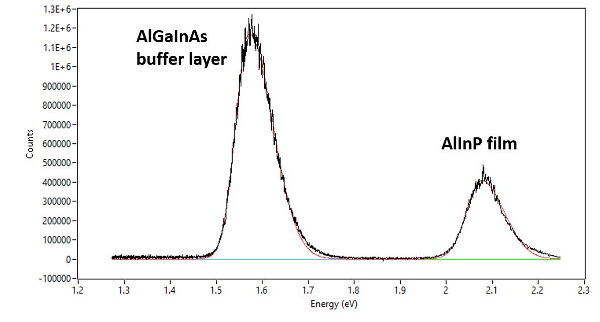
Typical PL spectrum (black) and the resulting fit (red) for the AlInP sample. The band gap PL signals from both the film and the underlying buffer layer are clearly distinguishable.
The PL intensity of the AlInP film was found to be inversely related to the emission energy of the underlying buffer layer. The localized reduction in PL intensity was determined to be due to localized changes in the band gap of the buffer layer reducing the available carriers for radiative recombination.
Sample courtesy of Dr. Kirstin Alberi of the National Renewable Energy Laboratory.
Measurements were taken with a Klar Mini Pro instrument using 532 nm laser excitation and 0.6 micron spatial resolution for a total of 695,556 spatial (x,y) points. A PL spectrum was collected at each (x,y) point. The PL measurements showed distinct band gap emissions from both the film and the buffer layer.
Using KlarFit, the resulting spectra were fitted to a model of two bigaussian functions. The fitted peak parameters, such as peak energy, were then plotted as a function of spatial position (x,y) to produce PL maps. This method allows extraction and comparison of the spatial relationships between different peak parameters. The figure below shows the comparison for the buffer layer peak (left) and the AlInP film (right). Direct and exact comparisons between the buffer layer properties and the AlInP film properties can be made.

Peak parameters as a function of spatial coordinates. The left side presents the intensity and energy maps for the AlGaInAs buffer layer emission, while the right side presents the same for the AlInP film emission. Total area is 0.5×0.5 mm.
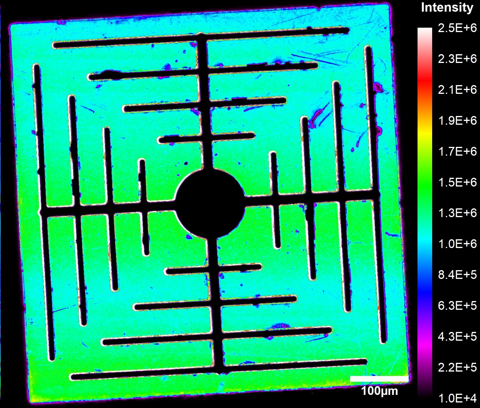
Here a commercial yellow LED was studied with PL mapping. Measurements were taken over the entire die, with 0.5 micron spatial resolution and a total of 2 million spatial points. A plot of intensity is shown on the right. The intensity of the PL peak at 2.1 eV showed variations across the die (black regions correspond to electrical contacts).